Product
 Brand
Brand Articles
 Tools
Tools
SRAM vs DRAM: Key Differences and Applications Guide
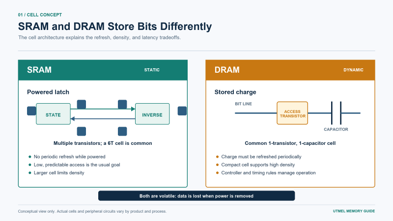
SRAM and DRAM are both volatile random-access memories, but they solve different system problems. SRAM uses a latch-based cell that holds its state while power is present and does not need periodic refresh. DRAM stores charge in a compact cell and must refresh that charge, which enables much higher density but adds controller and timing requirements.
The practical choice is rarely "which technology is better?" A useful design decision starts with capacity, latency, bandwidth, access pattern, controller support, power states, reliability, package, temperature range, lifecycle, and cost. The exact device datasheets and the processor or FPGA memory-controller documentation remain the final authority.
Quick answer
Choose SRAM when the working set is relatively small and low, predictable access latency is more important than capacity or cost per bit.
Choose DRAM when the system needs substantially more working memory and can support DRAM initialization, timing, refresh, and signal-integrity requirements.
Do not compare technologies from a single speed number. SRAM access time, DDR transfer rate, DRAM read latency, bus width, burst length, bank behavior, and controller overhead describe different parts of performance.
Do not assume one technology is a drop-in replacement for the other. The interface, voltage, package, timing model, controller, PCB layout, initialization, and software behavior can all change.
| Design question | SRAM | DRAM |
|---|---|---|
| How is a bit held? | A powered latch made from multiple transistors; six-transistor cells are common | Commonly one access transistor and one storage capacitor |
| Periodic refresh | Not required while power is maintained | Required because stored charge leaks over time |
| Volatile | Yes | Yes |
| Typical strength | Low and predictable access latency | High density and large capacity |
| Typical system role | Processor cache, scratchpad, lookup table, FIFO, packet buffer, embedded working memory | Main memory, graphics memory, mobile working memory, high-bandwidth accelerator memory |
| Common interfaces | Embedded SRAM, asynchronous parallel SRAM, synchronous SRAM | SDRAM families such as DDR, LPDDR, GDDR, and HBM |
| Main implementation concern | Capacity, access time, standby/active current, bus timing, package | Controller compatibility, timing set, refresh, training, layout, power integrity, thermal behavior |
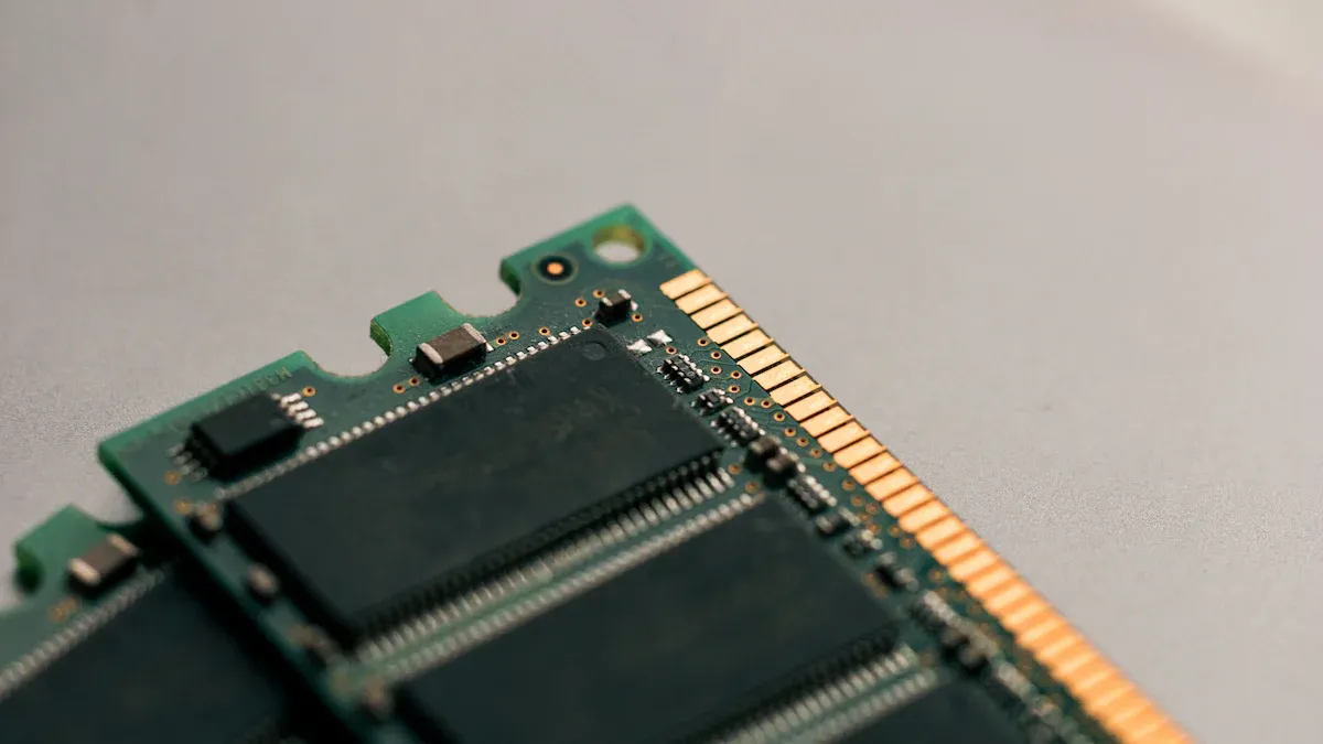
What is SRAM?
Static random-access memory stores each bit in a bistable circuit. A common CMOS SRAM cell uses six transistors, although other cell topologies exist. Once written, the cell keeps its logical state as long as its supply remains within specification. It does not need the periodic row refresh used by DRAM.
"Static" does not mean nonvolatile. Ordinary SRAM loses its contents when power is removed. Battery-backed SRAM, nonvolatile SRAM, and EERAM products add retention mechanisms that are outside the behavior of ordinary SRAM.
SRAM also describes more than one interface. Embedded SRAM may sit inside a microcontroller, processor, FPGA, or ASIC. Standalone asynchronous SRAM responds to address and control signals without a bus clock. Synchronous SRAM uses a clocked protocol to increase throughput. These implementations differ substantially in density, timing, power, and system integration.
Common SRAM roles include:
processor caches and tightly coupled memory;
deterministic scratchpad memory in real-time systems;
packet buffers and lookup tables in networking equipment;
FIFOs, frame or line buffers, and temporary working storage;
battery-backed event logs when the chosen device and circuit support that mode.
What is DRAM?
Dynamic random-access memory commonly stores a bit as charge in a one-transistor, one-capacitor cell. The charge decays, so rows must be refreshed periodically. Read operations also involve sensing and restoring the stored state. These requirements are handled by the DRAM device together with a compatible memory controller.
The compact cell is the foundation of DRAM's density advantage. That advantage makes DRAM practical for large working-memory capacities in computers, servers, mobile devices, graphics systems, and accelerators.
Modern DRAM is a family of technologies rather than one interchangeable interface:
DDR SDRAM is widely used for system memory.
LPDDR is optimized for mobile and other power-sensitive systems.
GDDR is designed for graphics and high-throughput workloads.
HBM uses stacked DRAM and a very wide interface for high aggregate bandwidth.
Each generation and family has its own signaling, voltage, package, timing, initialization, and controller requirements. A high transfer rate does not by itself describe first-access latency or application performance.
SRAM vs. DRAM: the differences that matter
Refresh and predictability
SRAM avoids periodic refresh, which can make its access behavior easier to bound. This is valuable in caches, real-time buffers, and other paths where worst-case latency matters.
DRAM refresh consumes time and energy, but refresh is only one part of DRAM behavior. Row activation, precharge, bank state, burst transfers, controller scheduling, and contention also affect observed latency. Controllers can overlap or schedule operations, so application performance cannot be predicted from a refresh interval alone.
Latency and bandwidth are not the same
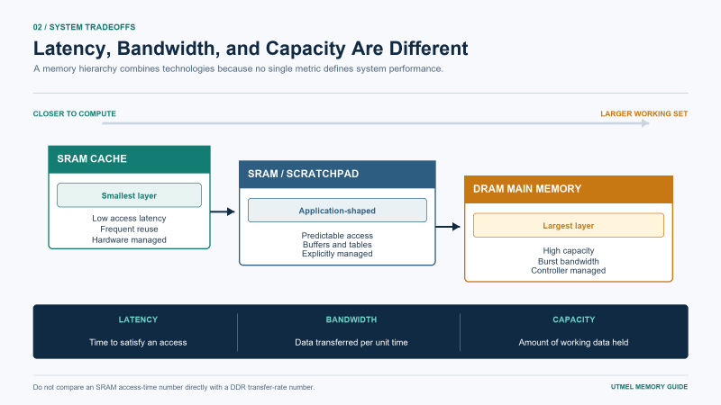
SRAM is generally selected for lower access latency. DRAM is generally selected for capacity and can deliver high sequential or parallel bandwidth through modern interfaces. This is why a processor can use SRAM-based cache close to the cores while using DRAM as much larger main memory.
A comparison such as "10 ns SRAM versus 60 ns DRAM" is not a technology law. It may compare an asynchronous SRAM access-time specification with a particular DRAM random-access sequence, while ignoring transfer rate, burst length, bus width, cache behavior, and controller policy. Compare the actual path the application will use.
Density, capacity, and cost
The common DRAM cell uses fewer active storage devices than a conventional SRAM cell. This supports higher bit density and usually lowers cost per bit at large capacities. SRAM's larger cell is the tradeoff for avoiding refresh and achieving low access latency.
Cost must still be evaluated at the system level. A small SRAM may eliminate an external controller or simplify timing. A large DRAM may require a more capable processor, additional power rails, controlled-impedance routing, training support, and more validation. The lowest component price is not always the lowest implemented cost.
Power is workload-specific
It is unsafe to say that SRAM always uses less power or that DRAM always uses more. SRAM has no refresh current, but SRAM leakage can become important as capacity grows. DRAM includes refresh power, yet power-saving and self-refresh modes can reduce consumption in suitable operating states. I/O switching, bus width, data rate, voltage, activity, temperature, controller policy, and memory utilization all matter.
Use the selected device datasheet and the manufacturer's power model with realistic read, write, idle, and low-power duty cycles. Keep standby power and active energy per transferred bit as separate questions.
Where SRAM and DRAM fit in a system
A typical processor-based system uses several memory layers. Small SRAM structures close to execution units hold frequently accessed instructions and data. Larger DRAM capacity sits behind a memory controller. Software usually sees the cache hierarchy and main memory as one addressable system, while hardware moves data between layers.
This coexistence is the important design pattern. SRAM does not need to replace DRAM to improve performance, and DRAM does not need to replace SRAM to increase capacity. Each layer is sized and controlled for a different purpose.
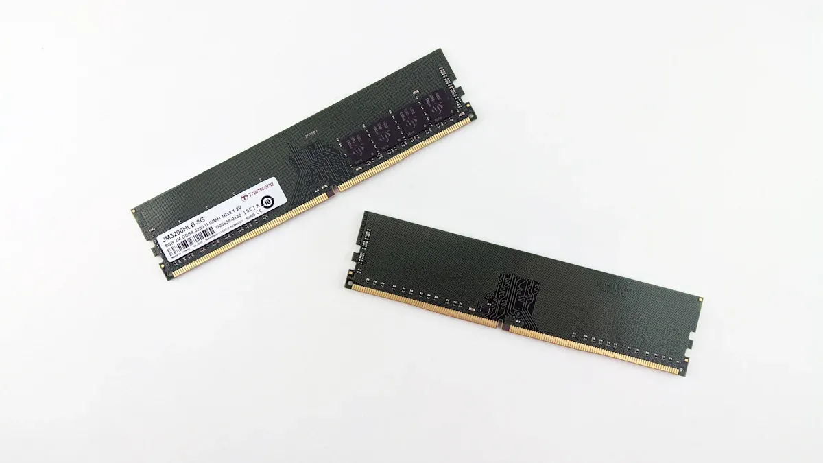
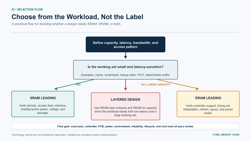
How to choose between SRAM and DRAM
1. Define the memory's role
Decide whether the memory is a cache, scratchpad, frame buffer, packet buffer, program working area, main memory, or accelerator data store. The role determines whether predictable latency, capacity, sequential bandwidth, random access, or retention during a low-power state is most important.
2. Quantify capacity and traffic
Record minimum capacity, bus width, peak and sustained bandwidth, read/write ratio, burst length, random-access rate, and worst-case latency. Include protocol overhead and simultaneous masters. A nominal memory data rate is not the same as usable application bandwidth.
3. Check controller and interface support
For SRAM, verify asynchronous or synchronous timing, voltage levels, control signals, bus turn-around, and wait-state requirements. For DRAM, verify that the processor, FPGA IP, or memory controller supports the exact DRAM family, generation, density, device width, ranks, timing parameters, and initialization flow.
4. Build a realistic power budget
Model active reads and writes, idle periods, refresh or self-refresh, standby modes, I/O termination, temperature, and utilization. Use the manufacturer's calculator when one is available, then validate the estimate on representative hardware.
5. Review reliability and environment
Check operating temperature, supply tolerance, ECC or parity requirements, soft-error goals, data integrity during reset or brownout, and qualification needs. "SRAM" or "DRAM" alone does not establish an automotive, industrial, medical, or aerospace qualification level.
6. Confirm package and lifecycle
Verify package, pinout, PCB routing, signal integrity, power integrity, thermal design, lifecycle status, PCN/EOL process, and authorized sourcing. Memory substitutions require the same discipline as other component changes.
Common selection mistakes
Comparing SRAM access time directly with DDR transfer rate.
Treating refresh as the only contributor to DRAM latency or power.
Assuming all SRAM uses the same cell, interface, or standby behavior.
Assuming every DRAM family is electrically or mechanically compatible.
Choosing from capacity and price before checking controller and PCB support.
Treating a wider temperature range as proof of qualification.
Approving a substitute without validating the exact ordering code and system behavior.
FAQ
Is SRAM always faster than DRAM?
SRAM generally offers lower access latency and is commonly used where predictable, rapid access matters. However, "faster" must be defined. A modern DRAM interface may provide very high burst bandwidth, while an SRAM may excel at random access. Compare complete devices and system paths, not technology names alone.
Why does DRAM need refresh?
The charge stored in a DRAM cell decreases over time. Periodic refresh restores that state before it becomes unreliable. The controller and DRAM timing rules determine how refresh is scheduled.
Does SRAM keep data when power is removed?
Ordinary SRAM does not. It is volatile. Products described as battery-backed SRAM, nonvolatile SRAM, or EERAM add a backup supply or nonvolatile storage mechanism and must be evaluated as separate device classes.
Why is DRAM used as main memory?
Its compact cell supports high density and large capacities at practical cost per bit. Modern DRAM families also provide the bandwidth needed by processors, graphics devices, and accelerators when paired with a compatible controller.
Which memory matters more for gaming?
They serve different layers. Processor and GPU caches typically use SRAM internally, while system memory and graphics memory use DRAM families. A platform designer or buyer usually selects platform-supported DRAM capacity and speed; the cache architecture is built into the processor or GPU.
Can SRAM replace DRAM, or can DRAM replace SRAM?
Not as a general drop-in change. The technologies differ in capacity, interface, timing, voltage, package, controller requirements, PCB design, and software behavior. A replacement is possible only when the complete system is redesigned or the exact alternative is explicitly supported and validated.
Official references
Related Utmel resources
 UTMEL
UTMEL
We are the professional distributor of electronic components, providing a large variety of products to save you a lot of time, effort, and cost with our efficient self-customized service. careful order preparation fast delivery service
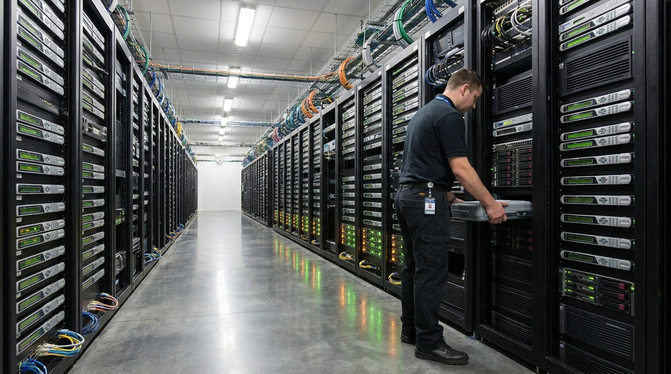 High-Capacity HDDs in the AI Era: Sourcing Massive Storage for Cold DataUTMEL04 July 2026578
As generative AI and LLMs drive an explosion of unstructured data, high-capacity enterprise HDDs remain the most cost-effective solution for cold storage. Despite rising prices and supply chain bottlenecks, mechanical drives offer a massive cost-per-gigabyte advantage over SSDs. Technologies like HAMR and SMR enable capacities beyond 24TB, though deploying these drives requires robust RAID 6 strategies and secured IC supply chains to mitigate rebuilding and procurement risks.
Read More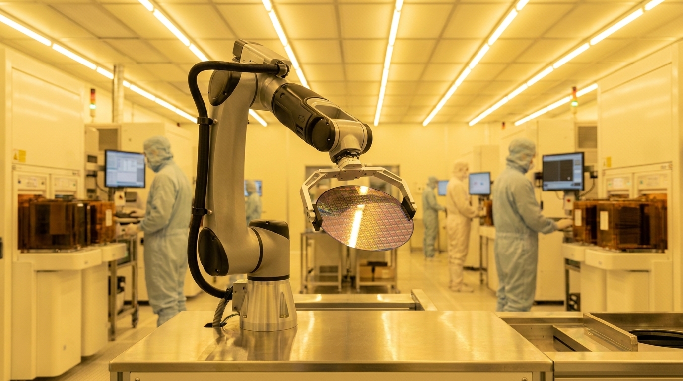 LPDDR5 Memory 2026: Lead Times, HBM Impact, and Procurement StrategiesUTMEL17 July 20263577
Global semiconductor fabrication facility managing advanced memory production. In Q2 2026, contract prices for 12GB LPDDR5X modules surged 89% quarter-over-quarter, jumping from $77.10 to $145.90, while lead times for advanced memory components stretched to 40–58 weeks. A vehicle platform designed in 2023 with specific memory requirements must ship in 2026, regardless of spot market conditions.
Read More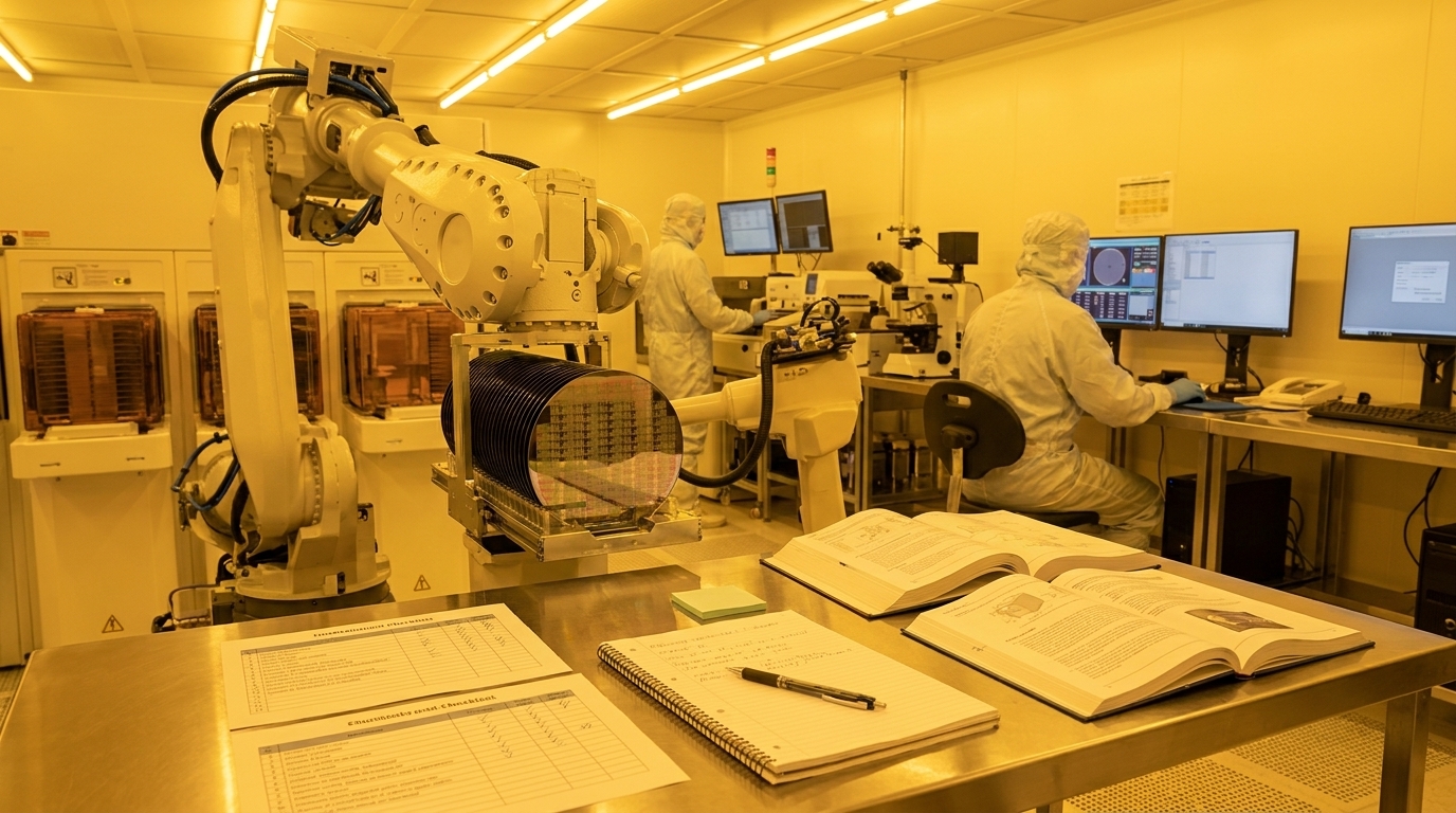 2026 DRAM and the 3-to-1 HBM Rule: Market Supply Analysis and B2B Procurement GuideUTMEL23 July 20264305
This technical report explains how the physical "3-to-1 wafer penalty" of High Bandwidth Memory (HBM) production has cannibalized standard DRAM capacity, causing severe shortages of DDR4 and DDR5 in 2026. As major hardware OEMs pass these soaring component costs directly to enterprise buyers, procurement teams must abandon Just-in-Time models in favor of rolling safety stocks and strategic long-term distributor agreements to protect budgets.
Read More Automotive vs. Industrial Memory: How to Verify Grade Codes Before Sourcing In this guideUTMEL06 August 2026349
Memory ordering codes can look almost identical while representing different temperature limits, packages, revisions, qualification evidence, or lifecycle commitments. For automotive and long-life industrial designs, the safe purchasing unit is the complete manufacturer ordering code, not a base part number plus a familiar-looking suffix.
Read More How to Use an External Hard Drive?UTMEL24 June 20219375
The external hard drive is a compact and portable hard drive storage which can be plugged in or unplugged at any time. It mainly uses USB or IEEE1394 interfaces. It can transmit data with the system at a higher speed. The IEEE 1394 interface transfer rate is 50-100 MB/s.
Read More
Subscribe to Utmel !
![22H240P.25]() 22H240P.25
22H240P.25Remington Industries
![34HNS2.5]() 34HNS2.5
34HNS2.5Remington Industries
![35HNSP.125]() 35HNSP.125
35HNSP.125Remington Industries
![40HNSP.5]() 40HNSP.5
40HNSP.5Remington Industries
![15HNSP.125]() 15HNSP.125
15HNSP.125Remington Industries
![21HNSP]() 21HNSP
21HNSPRemington Industries
![34HNS]() 34HNS
34HNSRemington Industries
![25HNSP.25]() 25HNSP.25
25HNSP.25Remington Industries
![23HNSP]() 23HNSP
23HNSPRemington Industries
![28H240P.25]() 28H240P.25
28H240P.25Remington Industries